凯瑞尔电子材料
1. Introduction
In the realm of Surface Mount Technology (SMT) packaging, carrier tapes serve as the backbone for transporting and protecting electronic components during assembly. The dimensional accuracy of carrier tapes directly impacts pick-and-place efficiency, component alignment, and overall yield. Among the various quality control measures, CCD (Charge-Coupled Device) automatic dimensional inspection has emerged as a critical technology for ensuring that carrier tapes meet stringent specifications. This article delves into the technical intricacies of CCD-based dimensional inspection, exploring its role in SMT packaging, the underlying product structure, process parameter control, common issues, quality standards, and selection guidelines. By leveraging advanced vision systems, manufacturers like Kairuie Electronic Materials Co., Ltd. achieve micron-level precision, enhancing reliability in high-volume production environments.
2. Product Structure & Material Composition
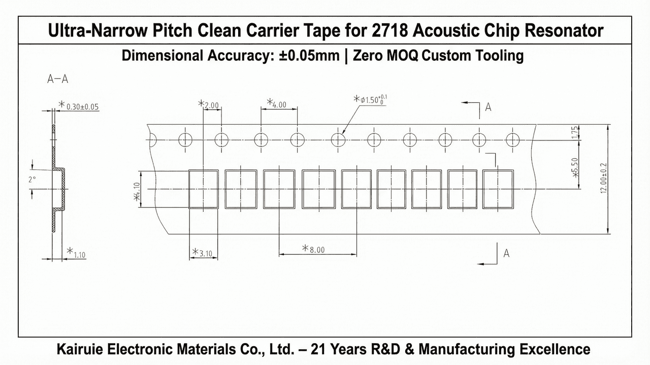
2.1 Layer Structure
Carrier tapes typically consist of three functional layers: a base layer (usually PET), an adhesive layer (for component retention), and an optional treatment layer (e.g., anti-static coating). The base layer provides mechanical strength and dimensional stability, while the adhesive layer ensures components remain securely in place during transport and feeding. The treatment layer may impart surface resistivity or other functional properties.
2.2 Key Material Parameters
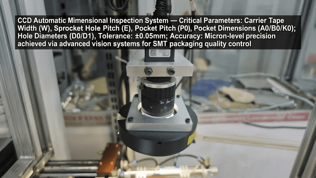
For the CCD inspection system, the critical parameters include carrier tape width (W), sprocket hole pitch (E), pocket pitch (P0), pocket dimensions (A0, B0, K0), and hole diameters (D0, D1). These parameters must be controlled within ±0.05mm tolerance to ensure compatibility with automated placement machines. The PET thickness typically ranges from 0.3mm to 0.5mm, with adhesive types selected based on component weight and environmental conditions. Surface resistivity is often specified at 10^6–10^9 Ω/sq for anti-static applications.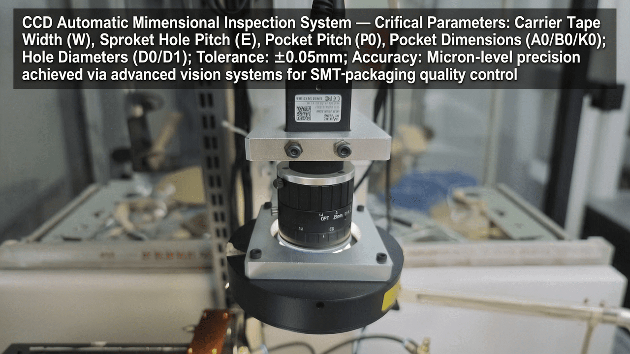
2.3 Product Models and Specifications
Kairuie’s CCD inspection system supports carrier tape widths from 8mm to 56mm (customizable to 88mm) and is compatible with both heat seal and self-adhesive sealing modes. The system achieves dimensional inspection accuracy of ±0.05mm for all critical parameters, including W, E, P0, P2, F, D0, D1, A0, B0, K0, and cumulative pitch P (per 10 pitches). This level of precision ensures seamless integration with downstream SMT processes.
3. Core Process Parameter Control
3.1 Temperature, Pressure, and Time
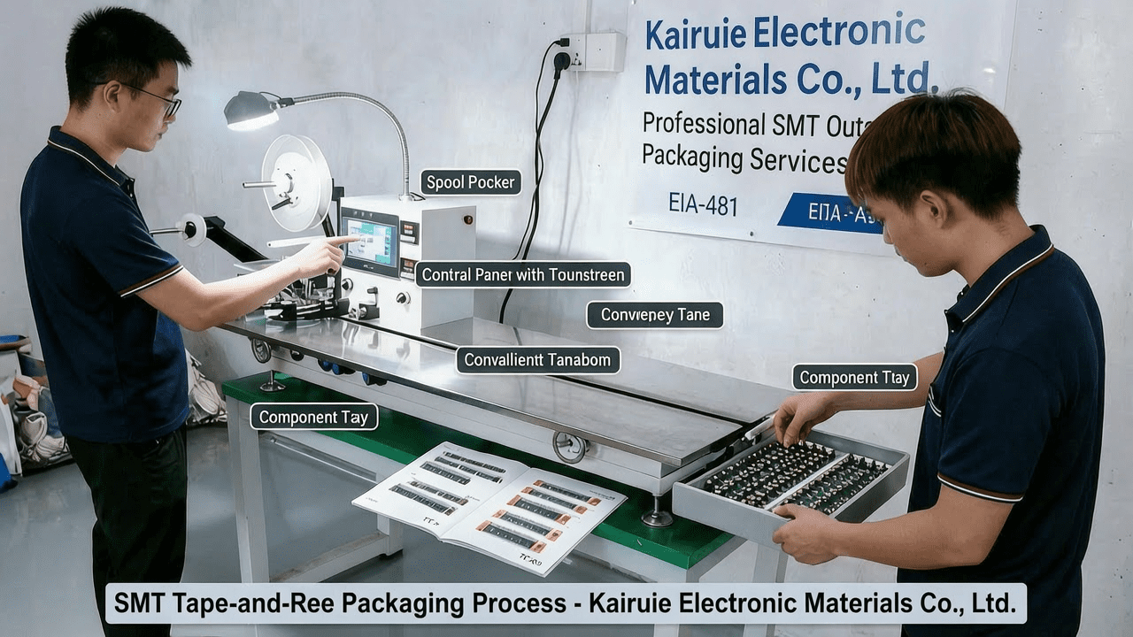
For heat seal applications, the recommended temperature range is 180–220°C, with pressure settings between 0.2–0.5 MPa and dwell time of 0.5–1.5 seconds. For self-adhesive mode, no heat is required, but pressure should be maintained at 0.1–0.3 MPa to ensure proper adhesion without deformation.
3.2 Impact on Quality
Temperature variations affect adhesive flow and bond strength; excessive heat may cause tape warping or adhesive oozing, while insufficient heat leads to weak seals. Pressure influences pocket formation and component seating; too high pressure can deform pockets, while too low pressure may result in loose components. Time controls curing and settling; inadequate time causes incomplete bonding, while excessive time reduces throughput.
3.3 Process Window Optimization
To optimize the process window, start with mid-range parameters (200°C, 0.35 MPa, 1.0 sec) and adjust based on visual inspection and peel strength tests. Use design of experiments (DOE) to identify interactions between parameters. For high-speed lines, reduce dwell time while increasing temperature slightly to maintain bond quality. Monitor cumulative pitch error (P) every 10 pitches to ensure consistent feeding.
4. Common Issues & Troubleshooting
| Symptom | Root Cause | Solution |
|---|---|---|
| Pocket deformation | Excessive pressure or temperature | Reduce pressure by 0.05 MPa or lower temperature by 10°C |
| Component misalignment | Incorrect pocket dimensions (A0/B0/K0) | Recalibrate CCD inspection; adjust die cutting parameters |
| Weak seal strength | Low temperature or short dwell time | Increase temperature by 10°C or extend dwell time by 0.2 sec |
| Sprocket hole elongation | Worn punch or misaligned die | Replace punch; realign die using CCD feedback |
| Cumulative pitch error >0.05mm | Thermal expansion or material stretch | Stabilize temperature environment; use low-shrinkage PET |
5. Quality Inspection Standards
5.1 Incoming Quality Control (IQC)
Visual inspection checks for scratches, contamination, and color consistency. Dimensional verification uses CCD to measure all critical parameters against specifications (±0.05mm). Peel strength testing ensures adhesive bonds exceed 0.5 N/cm for heat seal and 0.3 N/cm for self-adhesive.
5.2 In-Process Quality Control (IPQC)
Sampling frequency: every 1000 pockets or every 30 minutes, whichever comes first. Acceptance criteria: all dimensions within ±0.05mm, no visible defects, peel strength within limits. Reject any lot with >2% defects.
5.3 Reliability Testing
Aging test: 85°C/85% RH for 168 hours, then re-measure dimensions and peel strength. High/low temperature cycling: -40°C to +85°C for 100 cycles. Transportation simulation: vibration (10-500 Hz, 1.5g) and drop test (1m height). All tests must show no degradation beyond ±0.05mm or 10% peel strength loss.
6. Selection Guide
| Component Type | Recommended Product | Key Parameters | Application Scenario |
|---|---|---|---|
| 0402/0603 chips | 8mm carrier tape with heat seal | P0=4mm, A0=0.6mm, B0=0.8mm, K0=0.5mm | High-speed pick-and-place |
| QFP/BGA packages | 24mm carrier tape with self-adhesive | P0=12mm, A0=12mm, B0=12mm, K0=3mm | Large components, anti-static |
| LEDs/diodes | 12mm carrier tape with anti-static coating | P0=8mm, A0=3mm, B0=3mm, K0=2mm | Optical inspection, ESD protection |
| Connectors | 56mm carrier tape with heat seal | P0=16mm, custom pocket size | Custom shapes, high retention force |
7. Conclusion
CCD automatic dimensional inspection ensures carrier tapes meet the exacting demands of modern SMT assembly, providing micron-level precision and reliability. By integrating advanced vision systems with robust process control, Kairuie Electronic Materials Co., Ltd. delivers solutions that minimize downtime and maximize yield. For more information, visit www.kairuie.com. We invite industry peers to exchange ideas and explore collaborative innovations in SMT packaging technology.